Some people might read the title of this blog post and think “this sounds deeply sarcastic, who could think such a thing?” However, if you happen to be part of the group of people that finds these things fascinating, you know exactly how I feel.
The Satisfaction of Finishing a PCB Design is Hard to Explain…
This conglomeration of feelings is from pouring over documentation for days with the thought that at any moment, the parts you are researching could go out of stock due to supply chain issues. The feeling of finally identifying the perfect solution. The feeling of combining all your knowledge into something physical and shipping it off to get manufactured. And finally, the feeling of soldering on all the components to your PCB that just got mailed… hoping that by some miracle it works the first time.
It’s a massively complex puzzle with many pieces that you may not even realize that you are missing.
The Goalposts Keep Moving
Oddly enough, the fact that the plan has to continually adapt to a wide array of variables (available stock, the manufacturer, component types, and the requirements of whatever you’re designing for) is what makes PCB design so fun for me.
My particular set of constraints were as such:
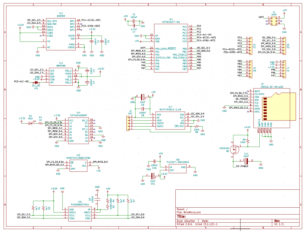
- Must have an IMU and Gyro
- Must have a microprocessor
- Must have externally facing pins
- Must have a DAC (digital to analog converter)
- Must have a micro SD card reader/writer
- Should have an altimeter
As a results of these constraints, an additional set of constraints could be generated
- Requirements were developed for each voltage level with required wattage (using the device data sheets)
- Logic level converters and voltage regulators were specked out (using the desired operating voltages)
An entire sheet of this data can be found here. There are some extraneous pages in there right now regarding a future project I’ll be working on, just refer to the “Smart Circuit BOM” page. It helped me roughly speck out various things and worked as a reference for all the data sheets.
An Iterative Process
A few redesigns had to be considered over the course of the board development
- IMU changed very far into development after I realized I had mistakenly assumed my first IMU had a gyro. This is probably the simplest and silliest error made throughout the project.
- The voltage level converters had to work under broad input levels. I didn’t realize this when designing the MISO line going to the microSD card. Originally my 3.3 volts was not going to trigger the input threshold of the voltage shifting device, but switching to TTL based chips fixed my issue as opposed to the CMOS chips I had originally been considering.
- I waited too long to buy something and it went out of stock so I had to switch the component. This was nearly the case for several other components, but I started biting the bullet and ordering before I could fully review a device’s data sheet.
It’s Been a Massive Learning Process
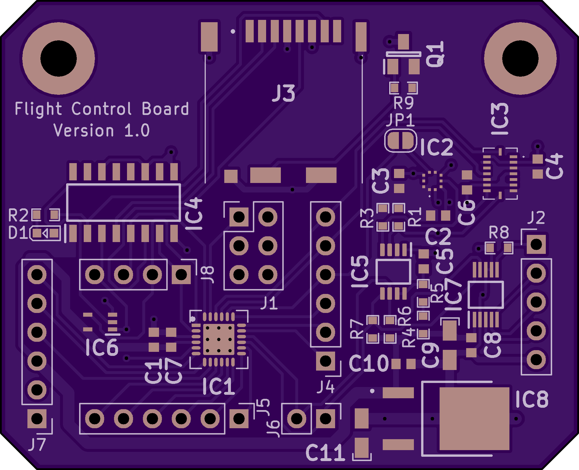
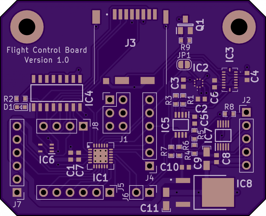
Doing everything in KiCad has not been the nightmare I thought it would be. I felt like it had a sharp learning curve when I first started, but because I’ve used it before, it wasn’t too hard. The hardest part of the project was actually the schematic design. However, after that, it was smooth sailing!
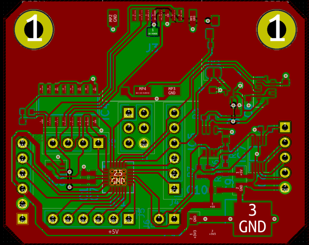
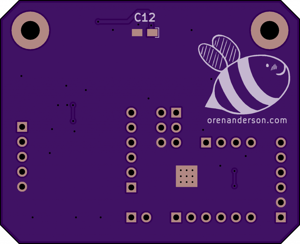
I didn’t have many concerns other that minimizing EMI (electromagnetic interference) at this point, so I made sure a ground pour took up nearly the entire bottom plane. I do not claim to understand EMI super well, but I believe this will help. To some degree, I also kept in mind common mode noise, but I figured I’d use what I had and just see how it performs.
Many of these terms (EMI, common mode noise, etc.) had been foreign to me before this project. A lot of the research I’ve done was just understanding all the small things I might not think about otherwise. Altium has some awesome videos on EMI that I watched and they helped me gain a new intuition on circuit design. I also read countless stack overflow posts and random articles that got me feeling confident about my design choices.
Conclusion of My PCB Design?
I think it would be a mistake to think that I’m done with this. In a few days time I’ll be receiving my PCBs as well as a stencil to help with applying some low temperature solder paste I purchased. I have some optimism with regards to everything working the first time, but I have the sneaking suspicion that something small was missed. We’ll see soon enough! This means the next step (after soldering!) is to attempt some programming on it. And after that? Well, maybe I’ll be able to add a few motor controllers and get it flying a drone! I guess we’ll see… If you’re interested in updates or downloading any of the files I’ve made, I’ll be posting everything to this GitHub repository. Hope to see you next month!